- 您现在的位置:买卖IC网 > Sheet目录2007 > MAX11040GUU+T (Maxim Integrated Products)IC ADC 24BIT 4CH 38-TSSOP
MAX11040K/MAX11060
24-/16-Bit, 4-Channel, Simultaneous-Sampling,
Cascadable, Sigma-Delta ADCs
16
Maxim Integrated
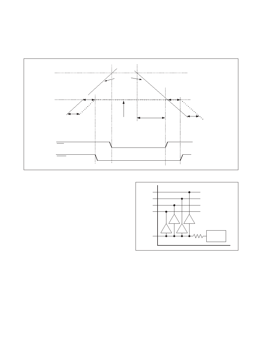
|AIN+ - AIN-|
FULL SCALE
(|0.88VREF|)
FAULT-DETECTION
THRESHOLD
(VPFT OR |VNFT|)
FAULT
OVRFLW
RECOVERY TIME
LATENCY
DIGITAL OUTPUT
DATA AT DOUT
LATENCY
Figure 5. Low-Frequency Analog Input Overvoltage Detection and Recovery
Reference
The devices operate with either a +2.5V internal
bandgap reference or an external reference source
between +2.3V and +2.7V applied at REFIO. Bypass
REFIO and each REF_ to AGND with a 1μF capacitor.
The reference voltage sets the positive and negative
full-scale voltage according to the following formula:
±FS = ±0.88 VREFIO
The reference voltage at REFIO (external or internal) is
individually buffered to generate the reference voltages
at REF0 to REF3 (see Figure 6.) These independent
buffers minimize the potential for crosstalk between
each of the internal ADCs.
Serial Interface
The devices’ interface is fully compatible with SPI/DSP
standard serial interfaces (compatible with SPI modes
CPOL = 1, CPHA = 0). The serial interface provides
access to four on-chip registers: Sampling Instant
Control register (32 bits), Data Rate Control register (16
bits), Configuration register (8 bits), and Data register
(96 bits). All serial-interface commands begin with a
command byte, which addresses a specific register,
followed by data bytes with a data length that depends
on the specific register addressed and the number of
devices cascaded (see Figures 7, 8, and the
Registers
section).
The serial interface consists of eight signals: CS,
SCLK, DIN, DOUT, CASCIN, CASCOUT, DRDYIN,
and DRDYOUT. CASCIN, CASCOUT, DRDYIN, and
DRDYOUT are used for daisy chaining multiple devices
together. See the
Multiple Device Connection section
for details on how to connect CASCIN, CASCOUT,
+2.5V
REFERENCE
REFIO
REF3
REF2
REF1
REF0
Figure 6. REFIO Input
发布紧急采购,3分钟左右您将得到回复。
相关PDF资料
MAX11046ECB+T
IC ADC 16BIT PAR 250KSPS 64TQFP
MAX11046ETN+T
ADC 16BIT SAMPLING 8CH 56-TQFN
MAX11049ECB+
IC ADC 16BIT PAR 250KSPS 64TQFP
MAX1104EUA+
IC CODEC 8BIT 8-UMAX
MAX11100EUB+
IC ADC 16BIT SRL 200KSPS 10UMAX
MAX11101EUB+
IC ADC 14BIT SRL 200KSPS 10UMAX
MAX11102AUB+
IC ADC 12BIT SPI/SRL 10UMAX-EP
MAX1111CPE+
IC ADC 8BIT LP 16-DIP
相关代理商/技术参数
MAX11040K
制造商:MAXIM 制造商全称:Maxim Integrated Products 功能描述:24-/16-Bit, 4-Channel, Simultaneous-Sampling, Cascadable, Sigma-Delta ADCs
MAX11040K_1111
制造商:MAXIM 制造商全称:Maxim Integrated Products 功能描述:24-/16-Bit, 4-Channel, Simultaneous-Sampling, Cascadable, Sigma-Delta ADCs
MAX11040K_12
制造商:MAXIM 制造商全称:Maxim Integrated Products 功能描述:MAX11040K Evaluation Kit/Daughterboard
MAX11040KDBEVKIT
制造商:MAXIM 制造商全称:Maxim Integrated Products 功能描述:MAX11040K Evaluation Kit/Daughterboard
MAX11040KDBEVKIT#
功能描述:数据转换 IC 开发工具 MAX5135/11040/11612 Eval Kit w/ FMC RoHS:否 制造商:Texas Instruments 产品:Demonstration Kits 类型:ADC 工具用于评估:ADS130E08 接口类型:SPI 工作电源电压:- 6 V to + 6 V
MAX11040KEVKIT
制造商:MAXIM 制造商全称:Maxim Integrated Products 功能描述:MAX11040K Evaluation Kit/Daughterboard
MAX11040KEVKIT#
功能描述:数据转换 IC 开发工具 MAX5135/11040/11612 Eval Kit w/ FMC RoHS:否 制造商:Texas Instruments 产品:Demonstration Kits 类型:ADC 工具用于评估:ADS130E08 接口类型:SPI 工作电源电压:- 6 V to + 6 V
MAX11040KGUU
制造商:MAXIM 制造商全称:Maxim Integrated Products 功能描述:24-/16-Bit, 4-Channel, Simultaneous-Sampling, Cascadable, Sigma-Delta ADCs